
Consultation Overview
Semiconductor Materials & Process Research Consultancy
Overview I provide specialised research consultancy and technical guidance in semiconductor materials, thin-film processing, surface chemistry, and semiconductor manufacturing technologies. My expertise includes Atomic Layer Deposition (ALD), Chemical Vapor Deposition (CVD), etching, surface treatment, thin-film deposition, materials selection, process optimisation, experimental design, and failure analysis. What I Can Help With ALD and CVD process development Thin-film deposition and surface chemistry Wet and dry etching concepts Etch selectivity and process optimisation Semiconductor materials and coatings Experimental design and process development Literature review and research-gap identification Process troubleshooting and root-cause analysis Materials characterisation strategy Research roadmap development Interpretation of experimental results Scale-up and process-validation strategy Who Can Benefit PhD scholars Master's students Research scientists Semiconductor engineers Materials scientists Academic researchers R&D professionals working on advanced materials and coatings Consultation Format 60-minute one-to-one online consultation. The session can include technical discussion, research planning, experimental strategy, literature guidance, and personalised recommendations. Important Note Consultancy is educational and technical in nature and is based on general scientific and engineering knowledge. No confidential, proprietary, or restricted industrial information will be disclosed. Pricing Single Session: ₹2,500 Full Research Project Support: ₹15,000–₹30,000, depending on scope and complexity.
Service Details
What's Included
- Video consultation
- Personalized guidance and advice
- Session notes and recommendations
- Follow-up support via email
Pricing Options
- Single Session ₹2,500
- Full Project ₹20,000
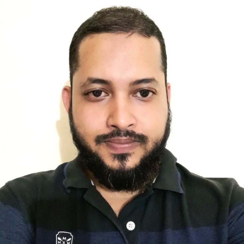
About Aminul Islam Sk
I have completed PhD in Chemistry from the Institute of Chemical Technology, Mumbai. My research focused on the synthesis of photoswitchable catalysts and their application to tune the kinetics of organic transformations via external stimuli such as light. After my PhD, I joined Applied Materials India Pvt Ltd as a research scientist. I have explored semiconductor surface engineering such as ALD, CVD, wet/dry/plasma etching, electro-driven etching, polishing, and deposition.
Experience
Research Proposal Development
Specialized expertise in research proposal development with 6 years of professional experience.